 Solid State Valve Power Supply Project - Initial Construction

 All photos copyright John Mills, last updated 27 Dec 2009


 The design of this PSU has slowly evolved over some six months of work. As this has tended to be a weekend / evening project
this is the reason for the time taken. My original thoughts came from an idea by Lee Bassett W3NLB in which he proposes a
solid state replacement for Filter Chokes. The original article can be found Here This gives the basics for a suitable HT supply,
allowing for currents up to 100mA. It soon became apparent from early bread boarding that serious amounts of heat were
needed to be dissipated in the pass transistor. Assuming a 375v DC input, if you require an output of say 90v @ 100ma, the
resulting wattage is 375 - 90 x 0.1 = 28.5W. It was for this reason I chose a large and thermally efficient heat sink for the 2 pass
transistors to be affixed to, and I also decided to make the DC input voltage to the regulators adjustable as well, leading to the
decision to use a multi - tapped secondary for my HT transformer. This allows the heat dissipation to be kept lower by keeping
the input voltage closer to the required output voltage. Next problem - where to purchase such an item ? Enquiries to a handful
of UK manufacturers met with little interest, or crazy prices.
So I turned to RS Components who were selling self -wind kits (182-9919). So, some 1500 turns of 0.25mm (33SWG) wire later, brought out to 8 taps gave me the
device I needed. Regrettably these have now been discontinued (probably due to H & S concerns) so it may be necessary to use a standard second hand
transformer and compromise on the voltage versus current drain. You may be able to persuade a local transformer supplier to let you have the pre-wound primary
bobbin along with the rest of the transformer to wind yourself, but it’s not very likely.
The front panel graphics were made using a dial drawing package and Paint Shop Pro, then printed to photo quality paper. To keep the printing clean, I laminated
the page using my office laminator. Next decision was not to have to all the control fixing nuts digging into the laminated panel, so I decided to make a sub - panel
for the majority of the controls. The laminated panel was then punched with the correct holes, and stuck to my 1.2mm thick aluminium front panel, after having
drilled that for the various pots, switches, panel meters and LED's etc. I then fabricated a circuit board to carry the LR8's along with the preset pots, and HT output
capacitors. This affixed to the rear of the switch sub panel using thread M3 spacers. Click on the images below to see a larger picture. Another excellent software
package for this is FrontDesigner3, available from Abacom
The design of this PSU has slowly evolved over some six months of work. As this has tended to be a weekend / evening project
this is the reason for the time taken. My original thoughts came from an idea by Lee Bassett W3NLB in which he proposes a
solid state replacement for Filter Chokes. The original article can be found Here This gives the basics for a suitable HT supply,
allowing for currents up to 100mA. It soon became apparent from early bread boarding that serious amounts of heat were
needed to be dissipated in the pass transistor. Assuming a 375v DC input, if you require an output of say 90v @ 100ma, the
resulting wattage is 375 - 90 x 0.1 = 28.5W. It was for this reason I chose a large and thermally efficient heat sink for the 2 pass
transistors to be affixed to, and I also decided to make the DC input voltage to the regulators adjustable as well, leading to the
decision to use a multi - tapped secondary for my HT transformer. This allows the heat dissipation to be kept lower by keeping
the input voltage closer to the required output voltage. Next problem - where to purchase such an item ? Enquiries to a handful
of UK manufacturers met with little interest, or crazy prices.
So I turned to RS Components who were selling self -wind kits (182-9919). So, some 1500 turns of 0.25mm (33SWG) wire later, brought out to 8 taps gave me the
device I needed. Regrettably these have now been discontinued (probably due to H & S concerns) so it may be necessary to use a standard second hand
transformer and compromise on the voltage versus current drain. You may be able to persuade a local transformer supplier to let you have the pre-wound primary
bobbin along with the rest of the transformer to wind yourself, but it’s not very likely.
The front panel graphics were made using a dial drawing package and Paint Shop Pro, then printed to photo quality paper. To keep the printing clean, I laminated
the page using my office laminator. Next decision was not to have to all the control fixing nuts digging into the laminated panel, so I decided to make a sub - panel
for the majority of the controls. The laminated panel was then punched with the correct holes, and stuck to my 1.2mm thick aluminium front panel, after having
drilled that for the various pots, switches, panel meters and LED's etc. I then fabricated a circuit board to carry the LR8's along with the preset pots, and HT output
capacitors. This affixed to the rear of the switch sub panel using thread M3 spacers. Click on the images below to see a larger picture. Another excellent software
package for this is FrontDesigner3, available from Abacom
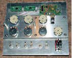
 Front Panel Begins...
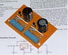
LR8 PCB
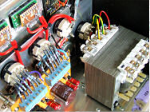
Taking shape.....
Further reading of some other forums concerning the LR8, led me to add a 10uF capacitor between the "adj" pin and ground, this was not indicated on the LR8
data sheet but was claimed to further reduce ripple on the output. I also decided to use N-Channel MOSFET's (STPNK50Z) in place of the original TIP50. Thus
the construction progressed and the final testing was ready. All seemed to work fine, except when switching voltage ranges there was a large lag before the output
voltage settled. This was obviously caused by the additional 10uF capacitor charging / discharging across the selected resistor for the appropriate range selected.
No problem, after waiting for everything to discharge, I simply snipped out the offending capacitor for each regulator. Yep ! the voltages soon changed now when
switching ranges until suddenly they stayed fixed at whatever the input HT supply was set at. First lesson learnt - switching the LR8 was obviously giving
sufficiently large spikes that the pass MOSFET promptly went short circuit Drain to Source, thus negating any control by the LR8. The LR8's responded to this by
drawing excess current and blowing the HT fuse.
Hasty mods followed:
1) Make the LR8 pluggable, achieved using small turned pin 2.54mm SIL sockets.
2) Replace the 10uF with a 1uF device to cut down the lag and also add a 470nF between the Gate and ground.
3) Having noted the MOSFET's seemed to blow easily on a previous bread board layout I decided to source a better NPN device. I chose a BUL38D, which has
the same min hfe of 10 as the TIP50, but looked to be a bit more rugged. PDF Data sheet is available Here
Front Panel Begins...
LR8 PCB
Taking shape.....
Further reading of some other forums concerning the LR8, led me to add a 10uF capacitor between the "adj" pin and ground, this was not indicated on the LR8
data sheet but was claimed to further reduce ripple on the output. I also decided to use N-Channel MOSFET's (STPNK50Z) in place of the original TIP50. Thus
the construction progressed and the final testing was ready. All seemed to work fine, except when switching voltage ranges there was a large lag before the output
voltage settled. This was obviously caused by the additional 10uF capacitor charging / discharging across the selected resistor for the appropriate range selected.
No problem, after waiting for everything to discharge, I simply snipped out the offending capacitor for each regulator. Yep ! the voltages soon changed now when
switching ranges until suddenly they stayed fixed at whatever the input HT supply was set at. First lesson learnt - switching the LR8 was obviously giving
sufficiently large spikes that the pass MOSFET promptly went short circuit Drain to Source, thus negating any control by the LR8. The LR8's responded to this by
drawing excess current and blowing the HT fuse.
Hasty mods followed:
1) Make the LR8 pluggable, achieved using small turned pin 2.54mm SIL sockets.
2) Replace the 10uF with a 1uF device to cut down the lag and also add a 470nF between the Gate and ground.
3) Having noted the MOSFET's seemed to blow easily on a previous bread board layout I decided to source a better NPN device. I chose a BUL38D, which has
the same min hfe of 10 as the TIP50, but looked to be a bit more rugged. PDF Data sheet is available Here